Introduction
The physical design of iot matters for every device that lives in the real world. A good design keeps the device working and safe. It balances size, cost, and function for real users. This guide explains the parts and choices that shape success. You will learn about sensors, printed circuit boards, power, and antennas. You will also see tips for testing, certification, and field service. I include simple checklists and tools to use. Each section uses short sentences and clear examples to keep things friendly. Read on to get practical steps you can apply to your next project.
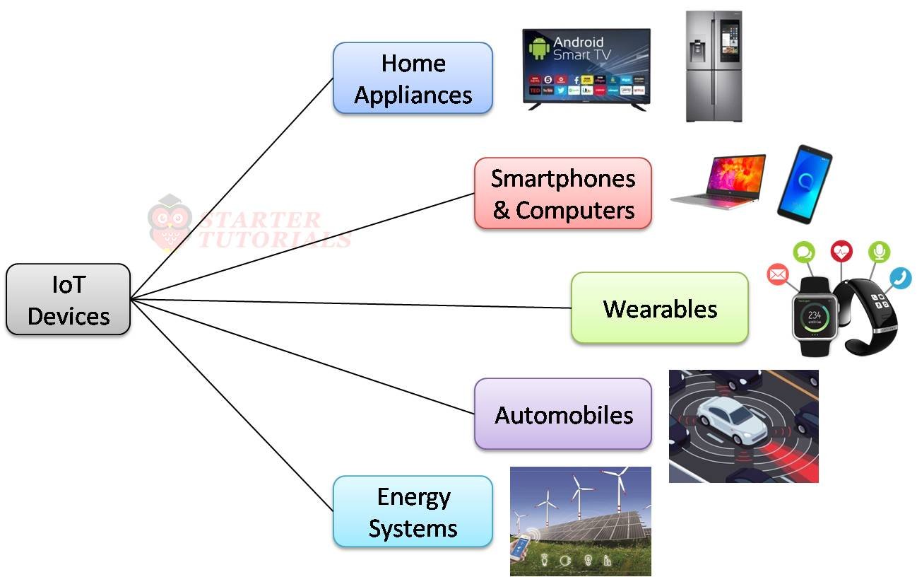
What is the physical design of IoT?
The physical design of iot covers the hardware that you can touch and fit into places. It includes sensors, actuators, controllers, batteries, and the printed circuit board. It also covers the enclosure, antenna placement, and wiring. The design defines how parts sit and how signals move between them. It determines how heat is handled and how water is kept out. The design must match the environment where the device will live. A phone on a desk has different needs than a sensor on a pole. Early planning reduces field failures and saves money on recalls.
Key components: sensors, actuators, and controllers
Start by listing the sensors and actuators the device needs. Sensors read light, temperature, motion, or moisture. Actuators open valves, move parts, or switch relays. Controllers run the code that reads sensors and drives actuators. The physical design of iot must place sensors where they will sense best. Avoid putting a temperature sensor near a hot chipset. Give actuators space to move and mount them securely. Pick controllers with the right I/O and low power modes. Early placement and part choice limit rework and speed the route to a working prototype.
PCB layout and electronic placement
A careful PCB layout makes the whole device behave better in the field. Keep power traces short and wide to reduce voltage drop. Place decoupling capacitors right at chip power pins. Separate noisy digital blocks from sensitive analog areas. Use ground planes to lower emission and improve signal return paths. Leave room for test points and connectors to help debugging. Think about the final enclosure and mechanical mounting when shaping the board. A good layout also simplifies assembly and raises production yield. Plan for controlled impedance for any fast signals.
Power management and battery life
Power design decides how long a device will run and how often you must service it. Choose the right battery chemistry and capacity based on duty cycle. Add efficient regulators and consider switching converters for higher efficiency. Use deep sleep modes in the MCU to save energy between events. Provide protection for over-current, reverse polarity, and deep discharge. If the device is rechargeable, include a safe charge controller and fuel gauge. Test battery life under real usage, not just in lab idle tests. The physical design of iot should make battery replacement or charging easy when needed.
Connectivity and antenna design
Radio performance often drives placement and case design. Wi-Fi, Bluetooth, LoRa, and cellular need different antenna areas and clearances. Keep antennas away from metal and large ground pours that detune them. Use matching networks to tune the antenna to the radio. Test the antenna on the real PCB inside the real enclosure, not just on a breadboard. Consider external antenna connectors if signal loss or orientation is a concern. The physical design of iot should allocate a radio-friendly zone in the case early in the project to avoid late rework.
Mechanical design and enclosure considerations
The enclosure protects electronics and determines mounting and user interaction. Choose materials by matching weight, strength, and cost needs. Plastic is light and cheap for many devices. Metal helps with ruggedness and thermal spreading. Design snap fits, screws, or gaskets to meet assembly and IP goals. Plan for easy access to batteries, SIMs, and service points if required. Make buttons and LEDs easy to use and see. The enclosure should also aid RF performance by leaving antenna zones clear. A well-thought-out enclosure reduces field failures and simplifies installation.
Thermal management and reliability
Heat shortens component life and alters sensor accuracy. Identify where heat will be produced. Use thermal vias and copper pours to spread heat through the PCB. Add thermal pads or heat sinks to chips that run hot. For sealed boxes, ensure conduction paths move heat to the case. Provide ventilation or conductive paths if needed. Test the device in hot and cold conditions to find weak points. The physical design of iot should include thermal margins and real-world tests to avoid surprises in the field.


EMC, EMI, and signal integrity
Electromagnetic noise can break radios and sensors. Use ground planes and good return paths for fast signals. Keep digital and analog routing separate and limit crossover. Add decoupling capacitors at each power pin and use ferrite beads on noisy lines. Add filters on power inputs and communication lines where needed. Consider shielding sensitive areas or noisy modules. Do simple pre-compliance checks early with prototypes. The physical design of iot must plan for EMC so that certification later is not a costly surprise.
Prototyping and manufacturing choices
Prototyping lets you test assumptions fast and cheaply. Use dev boards and 3D-printed enclosures to check fit and function. Move to small runs with a PCB house to validate assembly and test fixtures. Choose a contract manufacturer that has IoT experience. Design for assembly to reduce hand work and pick-and-place errors. Panelize boards for efficient production and plan solder mask and silkscreen details. Select parts with stock and supplier options to avoid sudden shortages. The physical design of iot benefits from manufacturer input early to save time and cost.
Testing, certification, and compliance
Testing proves a device meets rules and works where it must. Run functional tests for sensors and radios. Run environmental tests like vibration, humidity, and thermal cycling for devices in harsh places. Plan EMC and radio testing with a certified lab for FCC, CE, or local approvals. For battery-powered devices, include battery safety and transport compliance. Keep design files, BOMs, and test logs organized for audits. The physical design of iot should include certification timelines and budgets from the start, to avoid late-stage delays.
Security and physical hardening
Physical features can raise overall device security. Cover or hide debug ports when units ship. Add tamper switches or seals to detect opening. Use hardware secure elements to store keys safely. Design the boot flow so firmware updates require signed code. Protect SIM and SD slots from easy access. Think about how a thief might access the unit and make that harder. The physical design of iot is part of a layered security plan that pairs hardware hardening with strong software.
Cost, scaling, and supply chain planning
Design decisions affect unit cost and scale readiness. Pick components that are produced in volume and have long-term availability. Design a flexible BOM with approved alternates to handle supply issues. Standardize PCBs where multiple SKUs are needed to save tooling. Track lead times and minimum order quantities for key parts. Small changes in footprint or connector choice can cut production costs at scale. The physical design of iot must include supply chain planning to keep production steady.
Real-world examples and case study
I once led the physical design of iot for a soil moisture sensor project. The device needed five years of field life on a battery and reliable radio links. We chose low-power sensors and a small LoRa radio to stretch runtime. The device sent hourly reports and slept between transmissions. Early prototypes failed wind and rain tests and lost signal under tree canopy. We added a better seal, reinforced the mount, and offered an external antenna option. The final units ran two seasons without service calls. Field testing proved the fixes and increased customer confidence.
Best practices checklist for designers
Use a clear checklist to avoid missed steps during a project. Start with the exact use case and the operating environment. List the sensors, radios, and accuracy needs. Plan the pcb with power, ground, and RF zones. Design the enclosure for IP level, mounts, and thermal needs. Prototype and test thermal, vibration, and radio early. Add security features like tamper evidence and secure storage. Plan testing and certification timelines and budgets. The physical design of iot is much easier to control with a written checklist and versioned files.
Tools and resources for physical designers
Pick reliable tools to speed the work and find issues early. Use ECAD tools such as KiCad, Eagle, or Altium for PCB design. Use CAD tools like Fusion 360 for the enclosure and fit checks. Run thermal or RF simulation where it helps reduce prototype cycles. Equip a basic lab with a multimeter, regulated power supplies, and an oscilloscope. A spectrum analyzer is very useful for antenna tuning. Use 3D printing for fit checks and quick iterations. Online datasheets, vendor apps, and community forums are helpful learning sources.
Environmental and sustainability concerns
Think about the product lifecycle to lower environmental impact. Consider recyclable plastics or metals for the enclosure when possible. Design so common parts can be replaced without full scrappage. Choose batteries with responsible recycling paths. Optimize panelization and assembly to reduce waste. Document materials to meet regulations and eco-certifications. Consider repair paths and modular designs for upgrades. The physical design of iot can support a greener product lifecycle with small, practical choices.
Maintenance and field service planning
Good physical design reduces downtime and service cost. Design access for battery swaps, SIM changes, or sensor cleaning. Use modular subassemblies so field staff can swap a bad board quickly. Provide clear status LEDs or remote diagnostics to help troubleshooting. Create service guides with test points and expected readings. Test the ease of service with real technicians and refine instructions. The physical design of iot should include features for fast service to keep units running longer.
User experience and human factors
Devices must be easy to install and use for non-experts. Place LEDs, buttons, and labels where installers can see them on a ladder. Use tactile feedback for buttons and clear icons for ports. Make mounting systems simple and robust to avoid misalignment. Consider ergonomic shapes for handheld devices. Ensure the enclosure is safe to touch and free of sharp edges. The physical design of iot should reflect the installer and end user experience to reduce support calls and improve adoption.
Risk assessment and failure modes
Identify potential failure modes early and add mitigations. Evaluate battery failures, water ingress, antenna detachment, and connector fatigue. Use watchdog timers and graceful recovery for software faults. Design mechanical reinforcements where vibration is expected. Add redundancy for critical sensors when possible. Run worst-case scenario tests and document the results. The physical design of iot improves when risks are listed and verified through tests during development.
Manufacturing test and quality controls
Plan manufacturing tests that confirm each unit works before shipping. Add test points and design for easy fixture connection. Use automated optical inspection and selective x-ray for complex boards. Track yield and analyze failures to find systemic issues. Run burn-in tests for batches to catch early life problems. Keep firmware versions fixed during production runs to avoid mismatches. The physical design of iot needs strong QC processes to reduce warranty costs and customer returns.
Scaling from prototype to mass production
Scale carefully and validate every change before ramping production. Run pilot batches to confirm yields and assembly steps. Confirm suppliers and packaging for all production parts. Optimize the PCB for high-volume assembly and soldering. Automate testing with fixtures and software checks to speed throughput. Update documentation and version control for all revisions. The physical design of iot often needs small tuning to cut cost and boost yield at scale.
Future trends in the physical design of IoT
Expect more integrated modules that combine MCU, radio, and power management into single packages. Antenna-in-package and system-in-package solutions will simplify placement. Battery chemistry and charging tech will keep improving runtime slowly. Edge processing will change thermal layouts and reduce network needs. Recyclable materials and repairable designs will rise with new regulation and user demand. Staying current with new modules and test methods will shape future physical designs.
Conclusion
The physical design of iot blends electronics, mechanics, and real-world thinking into one plan. Good planning and early testing lower field failures and reduce support costs. Think about power, antenna, thermal, and security from the first sketches. Build quick prototypes and test them in the places where they will operate. Work with manufacturers and labs early to save time and money. Use the checklists and tools here as a starting point. Try a small project and apply these ideas. Share what you learn to help the next design go faster and stronger.
FAQs
How do I choose the best battery for my IoT device?
Choose a battery by capacity, voltage, and expected lifetime in your duty cycle. Compare chemistries like alkaline, lithium primary, and rechargeable lithium-ion. Think about temperature ranges and how the battery ages. For rechargeable systems, include a smart charge controller and fuel gauge. Test the battery under real load profiles to see true life. If the device is hard to access, prefer long-life primary cells or low-power designs. The physical design of iot is often limited by the battery, so plan battery and access early.
Do I always need external antennas for better range?
Not always. Internal antennas work well for short-range devices and controlled environments. External antennas help in weak-signal or obstructed sites. External antenna ports add assembly steps and cost and may require connectors and strain relief. Try internal and external antenna options during prototyping and measure link budgets. Keep antenna placement stable across all product variants. The physical design of iot should decide antenna type early based on field measurements.
What is the biggest thermal risk for sealed IoT devices?
Heat buildup is the biggest risk for sealed devices. Without airflow, components can run hotter than expected. This shortens battery life and can distort sensor readings. Use conduction paths, thermal vias, and copper pours to move heat to the case. Test prototypes in hot boxes and under direct sun to find hot spots. Choose components rated for the expected temperature extremes. The physical design of iot must include thermal testing to ensure reliability over years of use.
How early should I plan for testing and certification?
Plan testing and certification at concept and design stages. Certification labs need time and clear test plans, so schedule early. Different markets have different rules like FCC, CE, or local approvals. Factor these tests into your budget and timeline from the start. Keep detailed test records and versioned design files to support audits. The physical design of iot must include these milestones to avoid costly redesigns late in the project.
Can I retrofit security into an existing device design?
You can add some security upgrades, but hardware holes may remain. Firmware updates, secure boot, and encrypted communication help a lot. Adding a hardware secure element may require redesigning the PCB. Covering or sealing debug ports and adding tamper evidence can deter casual attackers. True hardware-level security works best when designed from the start in the physical design of iot. Retrofits can be helpful but are rarely as strong as a ground-up secure design.
What are simple tips to reduce EMI in my design?
Keep noisy traces short and route them away from sensitive analog paths. Use decoupling capacitors at every IC power pin. Add ferrite beads and LC filters on noisy supply lines. Use solid ground planes and avoid long loops in return paths. Shield noisy modules if needed and check connector routing. Run pre-compliance EMI tests early to catch issues while fixes are cheap. Small layout changes often fix big EMI problems and make certification easier.